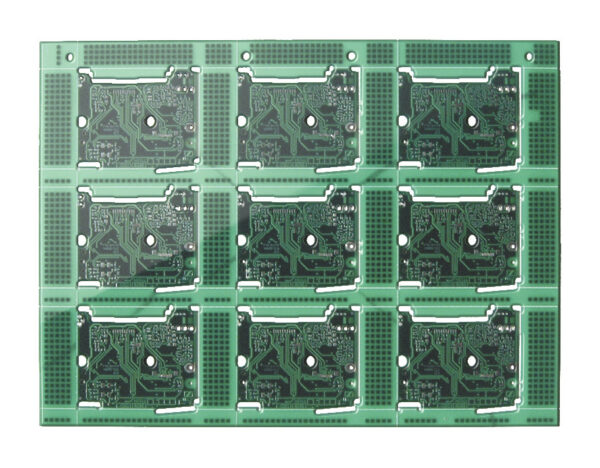
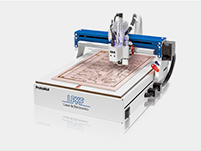
DOUBLE-SIDED PCB

Milling & Drilling Plotter

Manufacturing high-performance circuit boards from designs to finished PCB prototype in just a few hours

The versatile PCB circuit board plotters fit as tabletop systems into any development environment and cover the complete range from analog to RF applications.

The LPKF ProtoMat plotters are setting standards in precision, flexibility, and user-friendliness worldwide. The LPKF circuit board plotters are utterly irreplaceable for quick in-house production of printed circuit boards, whether for individual pieces in development projects or for low-volume production. They are ideal for high-performance, analog, digital, HF, and microwave applications.

Made in Europe: For more than three decades, LPKF circuit board plotters have been regarded as the benchmark in milling, drilling, and contour milling of circuit boards.

Every LPKF structuring system is delivered with an extensive software package that has been optimized for ease of operation, maximum quality, and fast delivery of results. LPKF CircuitPro imports all current CAD data and transmits the production data to the structuring systems.

ProtoMat S64

The basic system for almost all in-house PCB prototyping applications.

ProtoMat S104

Versatile high-end circuit board plotter for RF and microwave applications.
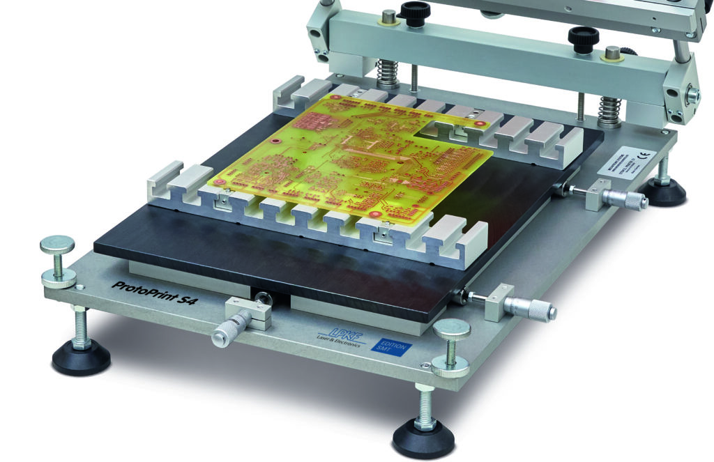
ProtoMat E44

The cost-effective entry into the world of professional in-house PCB prototyping.
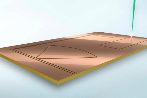
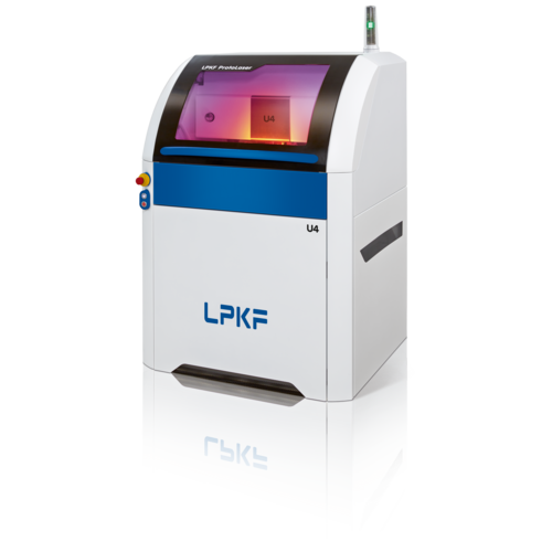
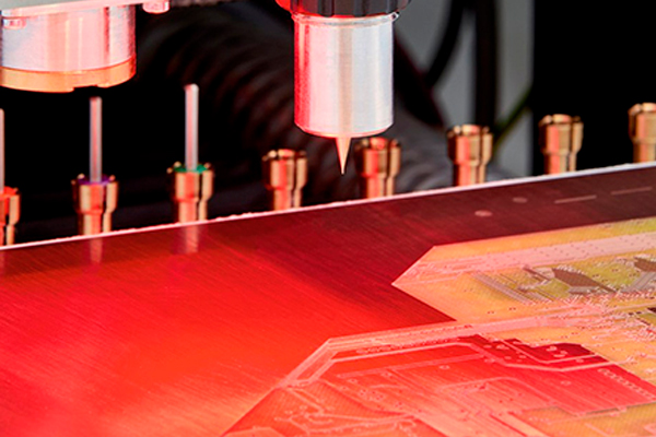
More information

Solder Mask & Print Screen

Laser structuring implements conductive paths even faster and more accurately than mechanical methods do. It places exact geometries on various substrates such as copper-clad FR4, aluminized PET film, ceramics, Duroid or PTFE.

The laser structuring process is predestined for manufacturing for HF and microwave applications. In comparisons with etched printed boards, laser-structured printed boards came out on top in terms of precision, repeatability, and agreement with simulation results.

The LPKF ProtoLaser plotters are compact and undemanding. They only require a power outlet and compressed air and can fit through any lab door. The LPKF ProtoLaser S4 and U4 are each equipped with a vacuum table and a vision system and meet the requirements of laser class 1 in operation (no additional protective measures necessary).

LPKF ProtoLaser U4

Thanks to the specific wavelength of the UV laser, the ProtoLaser U4 can structure, engrave and cut materials in a single operation. This laser system is stable in the lower power range so that even thin and organic layers can be processed with minimal heat transfer.
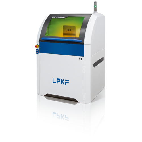
LPKF ProtoLaser R4

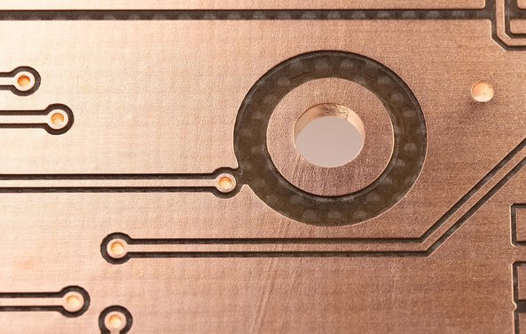
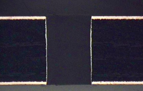
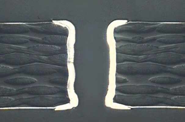
Laser ablation with practically no heat transfer: The shorter the processing pulse, the less heat is transferred to the adjacent material. The picosecond laser of the ProtoLaser R4 clears - an important hurdle falls: There is no more heat transfer to speak of, with the material struck by the laser evaporating right away.
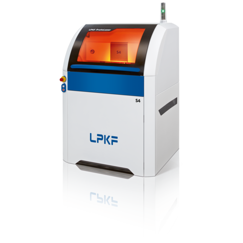
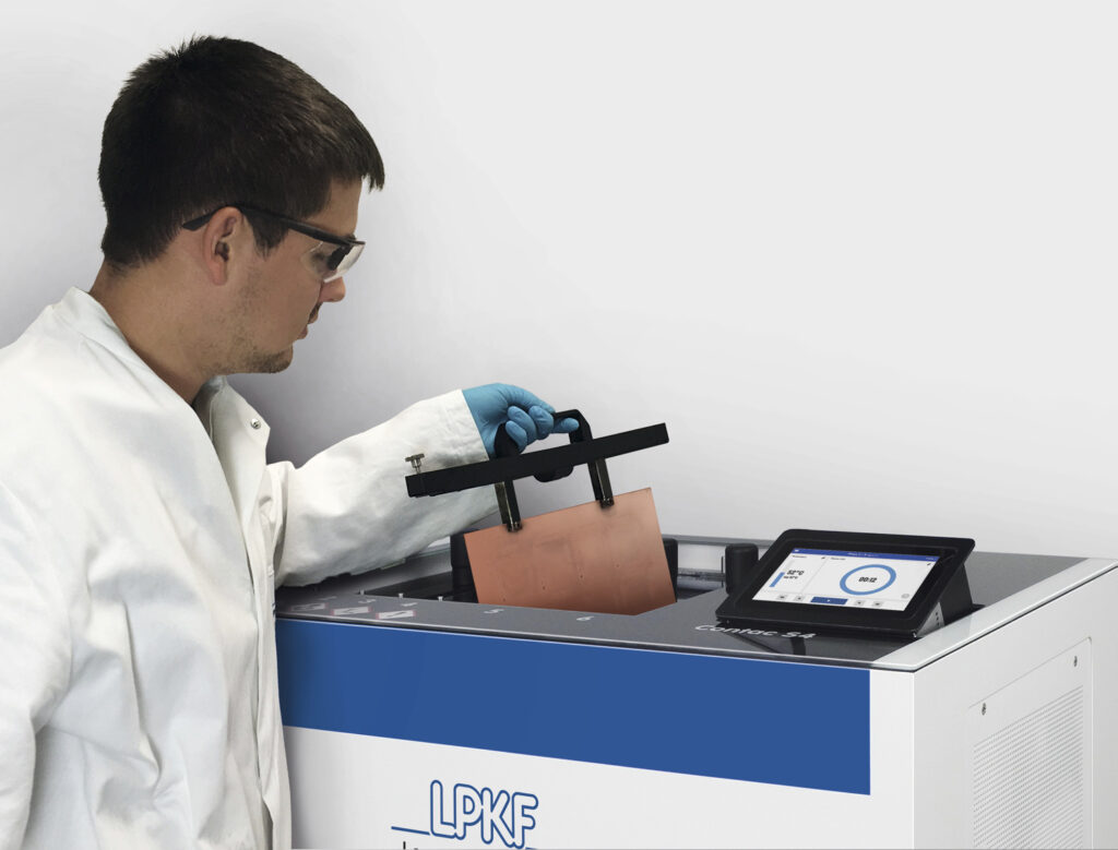
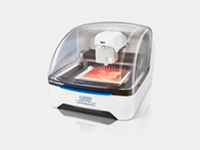
LPKF ProtoLaser S4

The compact laser system produces precise, fine structures for demanding PCBs in a very short time. Using a special process, the ProtoLaser S4 quickly removes large copper areas from laminated substrates such as FR4. The ProtoLaser S4 also delivers excellent results on special materials for RF applications.
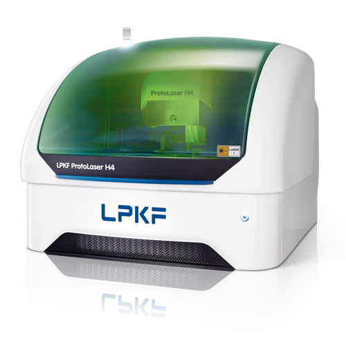
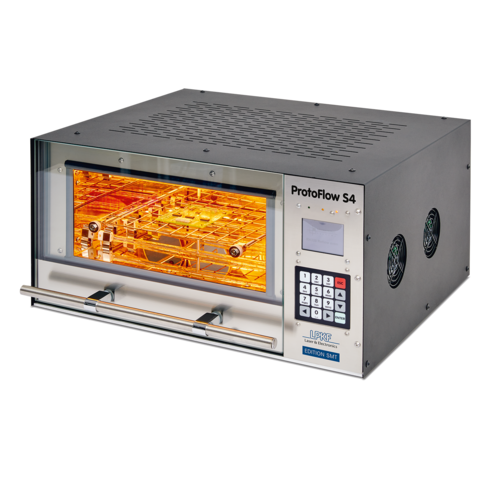
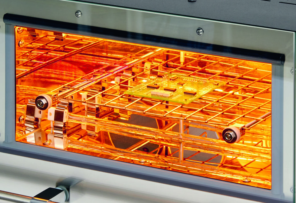
LPKF ProtoLaser H4

The Tabletop system enables efficient prototyping of digital and analog circuits, RF and microwave PCBs -- even for multilayer PCBs. It achieves precise geometries on virtually any material with the laser tool. Precise drilling and milling even of thick substrates using mechanical drilling.

More information

Through-hole Plating With Paste (Chemical Free)

Work with no chemicals

Through-hole Plating of Printed Circuit Boards For double-sided and multilayer printed circuit boards

LPKF ProConduct is handy, extremely fast and easy to use. All holes are plated through in a parallel process. This guarantees a safe, fast and temperature-resistant result.

Perfect result due to highly developed technology

The specially developed LPKF ProConduct through-hole plating process metallizes through-holes with a diameter of up to 0.4 mm and an aspect ratio of 1:4. Under special conditions, even holes with a smaller diameter can be through-plated. The electrical resistance of a fully plated through hole lies within a range of 10-25 m Ω. Even after 250 temperature change cycles, the resistance increases only slightly (max. 28 mΩ).

Through-hole Electroplating (Galvanized)

Through-hole plating for the lab
No knowledge of chemistry required

Reliable through-hole plating is a key to success with demanding PCB prototypes. The new LPKF Contac S4 combines various galvanic and chemical processes in a compact safety housing.

The connection of two or more layers is an indispensable part of PCB prototyping. The compact LPKF Contac S4 with six baths reliably performs this task: The board is routed through all stages of a bath cascade. In this way, homogeneous copper layers are produced on the walls of all through-holes, even with multilayer boards. The Contac S4 processes up to eight layers with a maximum aspect ratio of 1:10 (hole diameter to PCB thickness) and offers a final tin bath to protect the surface and improve solderability.

The powerful technology of the LPKF Contac S4 improves the build-up of the copper layer. Optimized anode plates and reverse pulse plating ensure uniform deposition, and activation via black hole technology, an integrated air flow and an additional process step for cleaning the through-holes provide secure connections to the surface copper without interfering interfaces. The result is uniform layer thicknesses in the holes and on the flat metal surface of the substrate.

Solder Mask & Print Screen

Two Usecases, One Solution

For years LPKF ProtoMat milling plotters have delivered excellent results in the production of printed circuit boards. LPKF offers two methods for professional surface finishing: solder resist with LPKF ProMask and assembly prints with LPKF ProLegend.

The solder mask coating protects the surfaces and conductive traces on a circuit board. Creation of short circuits between closely spaced pads is prevented by the professional surface finish applied in the soldering process.

LPKF ProMask is an easy-to-apply green solder mask. The professional surface finish is especially ideal for SMT prototypes with small trace spacings. LPKF ProLegend can apply any marking to the board – without using environmentally harmful wet chemical processes.

Solder Paste Stencil

Solder Paste Application

Application of solder paste on all pads on which components should be placed requires maximum precision. The LPKF ProtoPrint S4 stencil printer, a manual stencil printer for SMT prototyping and low-volume production, performs this task.

The mechanical resolution down to a grid size of 0.3 mm (12 mil) allows stencil printing in the ultrafine pitch range. The stencil thickness (between 100 µm and 250 µm) determines the amount of solder paste to be applied.

For PCB prototyping, milling of polyimide stencils with LPKF circuit board plotters is a genuine alternative to laser-cut steel stencils, especially from a cost perspective. Solder paste stencils (SMT stencils) can usually be milled in-house in less than ten minutes.

Reflow Oven

Reflow Soldering

The compact LPKF ProtoFlow S4 is the ideal reflow oven both for lead-containing and for RoHS-compliant lead-free reflow soldering, curing of the paste in the plated-through holes, and other thermal processes that need to be controlled precisely. The special “MultiZone” function allows the soldering process to be broken down into five separate phases, each with its own temperature profile. Four internal temperature sensors precisely control the temperature distribution over the entire board. The temperature data from the sensors are displayed on a monitor in temperature time graphs, which can be saved for later analysis.

The LPKF ProtoFlow S4 can be connected to a computer via a USB interface. The supplied intuitive PC software is used for recording temperature in real time and for programming and saving profiles. The LPKF ProtoFlow S4 can be equipped with a sensor module that records changes in temperature over time in up to four freely selectable positions – including on components.

Edasim, LLC Canada & United States

Edasim,LLC. 9100 Conroy Windermere RD Suite 200 Windermere, FL 34786,USA

+ 1 954 374 9125

+1 305 318 8775

edasim@edasim.com

MON - FRI 8:00 - 18:00